
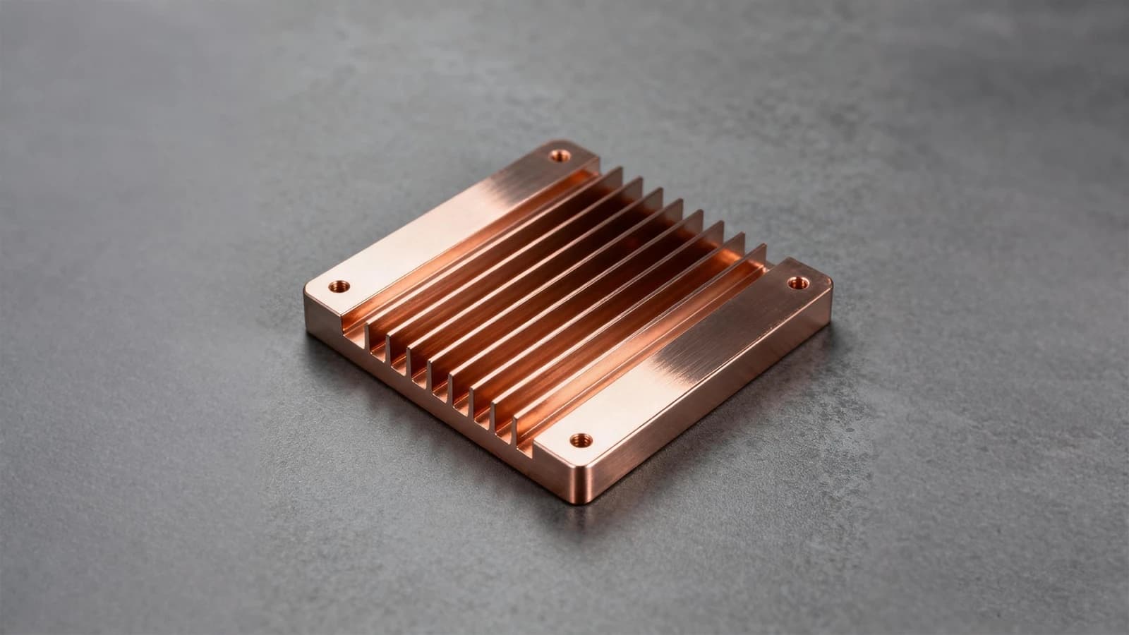
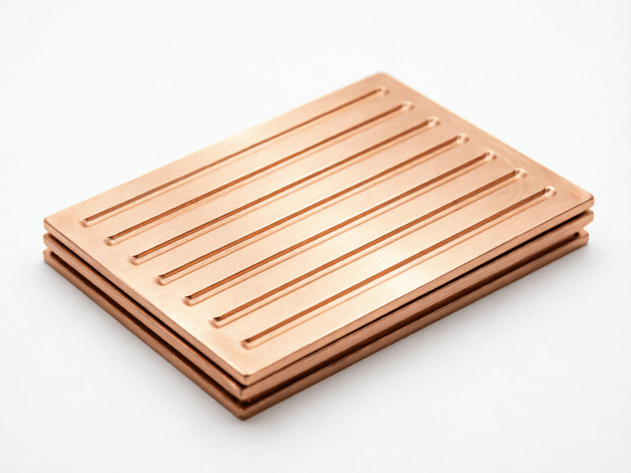
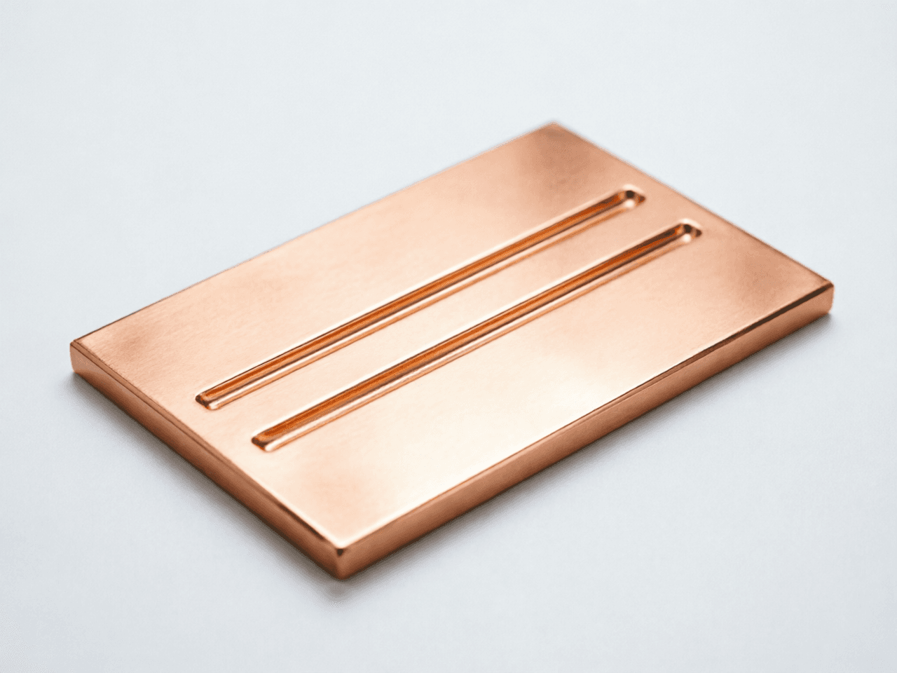
Tungsten Copper Thermal Substrate
High-density W–Cu heat spreading substrates for power & RF devices — PM sintering-infiltration plates, blocks and spreader blanks with tailored CTE, tight tolerances and minimal warpage for hermetic packaging.
- Materials
- Tungsten copper (W–Cu)
- Features
- High thermal conductivity, tailored CTE matching Si/GaN/GaAs/SiC, high-temperature stability, PM dimensional accuracy, Ni/Au plating & direct bonding compatible
- Application
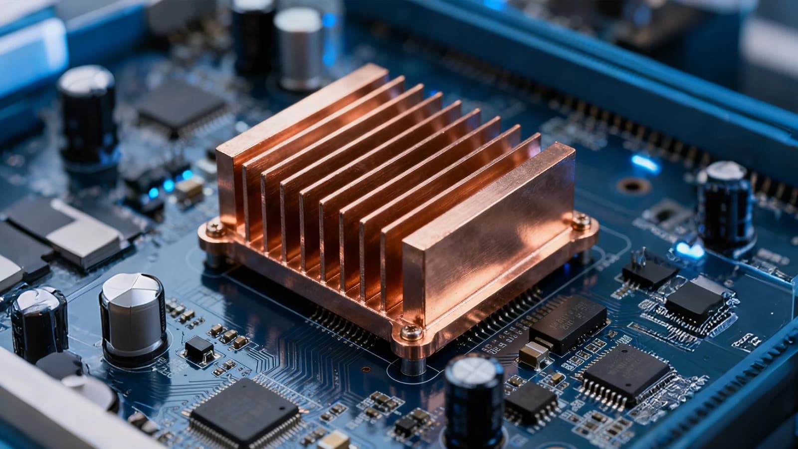
- Power semiconductor modules (IGBT, MOSFET, SiC/GaN), RF & microwave systems, high-power LED and laser bases, hermetically sealed aerospace/defense/industrial packages, precision electronics.
Frequently Asked Questions
What materials and process are used for Tungsten Copper Thermal Substrate?
Tungsten Copper Thermal Substrate is made from Tungsten copper (W–Cu) and is formed by MIM/PM (metal injection molding / powder metallurgy) near-net-shape and sintered to a relative density of ≥ 98%, which keeps mechanical properties close to wrought material.
What tolerances can Tungsten Copper Thermal Substrate hold?
Typical as-sintered dimensional tolerance is ±0.3–0.5% of the dimension. Tighter tolerances are achievable with secondary sizing or machining, agreed per part during quoting.
What is the MOQ and lead time for Tungsten Copper Thermal Substrate?
MOQ is 1000 pcs. Mold lead time is about 20 days (mold fee typically RMB 20–40k depending on part geometry), and production lead time is about 7 days once the mold is validated; secondary processing adds 3–5 days.
Related Products
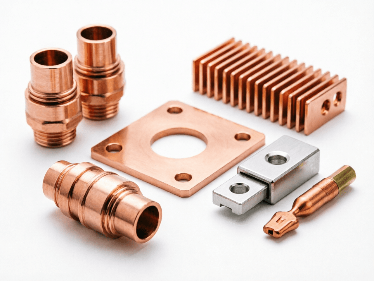
Copper Alloy MIM Parts
Materials: Copper, bronze, brass, tungsten copper
High thermal & electrical conductivity, bacteriostatic
View Details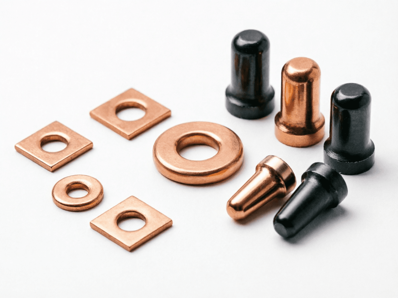
Tungsten Copper Precision Components
Materials: Tungsten copper (WCu), copper content 6–90%
Excellent arc erosion resistance, high conductivity, anti-adhesion, good machinability
View Details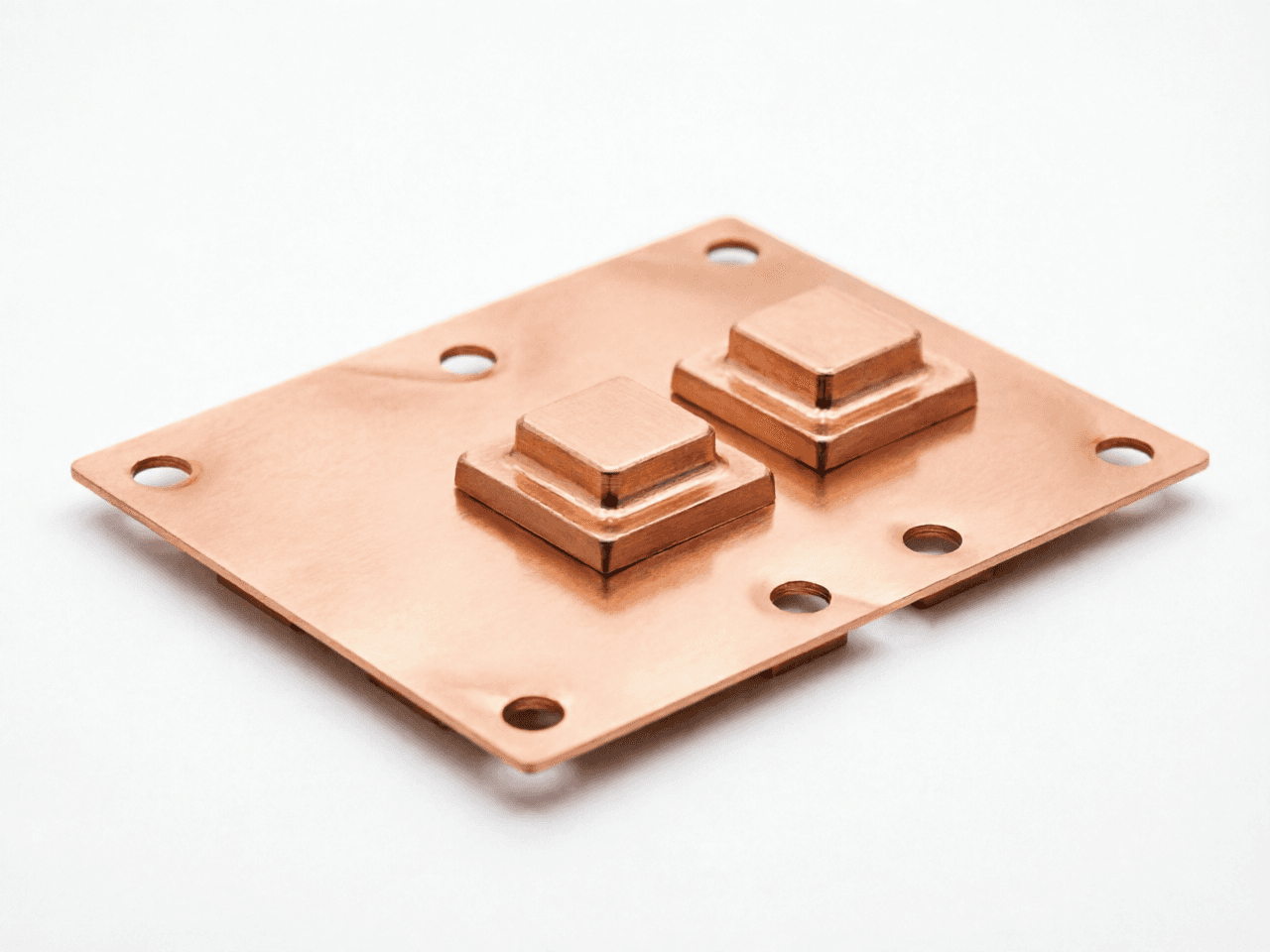
Copper Thermal Packaging Components
Materials: Pure copper, tungsten copper (W-Cu)
High thermal conductivity, CTE matching, low warpage, miniaturized complex geometries, plating/soldering/wire-bonding compatible
View Details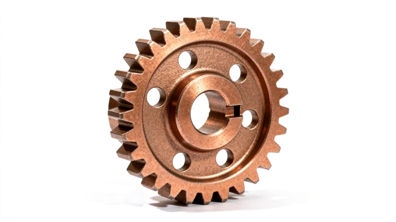
Copper Alloy Powder Metallurgy Gears
Materials: Copper-based PM alloys
Quiet meshing, controlled pore network for lubrication retention, high thermal stability, minimal post-machining
View Details