
Why Do EML/DFB Laser Submounts Use Tungsten Copper? Thermal Expansion Matching and Failure Modes
Published:
Why Do EML/DFB Laser Submounts Use Tungsten Copper? Thermal Expansion Matching and Failure Modes
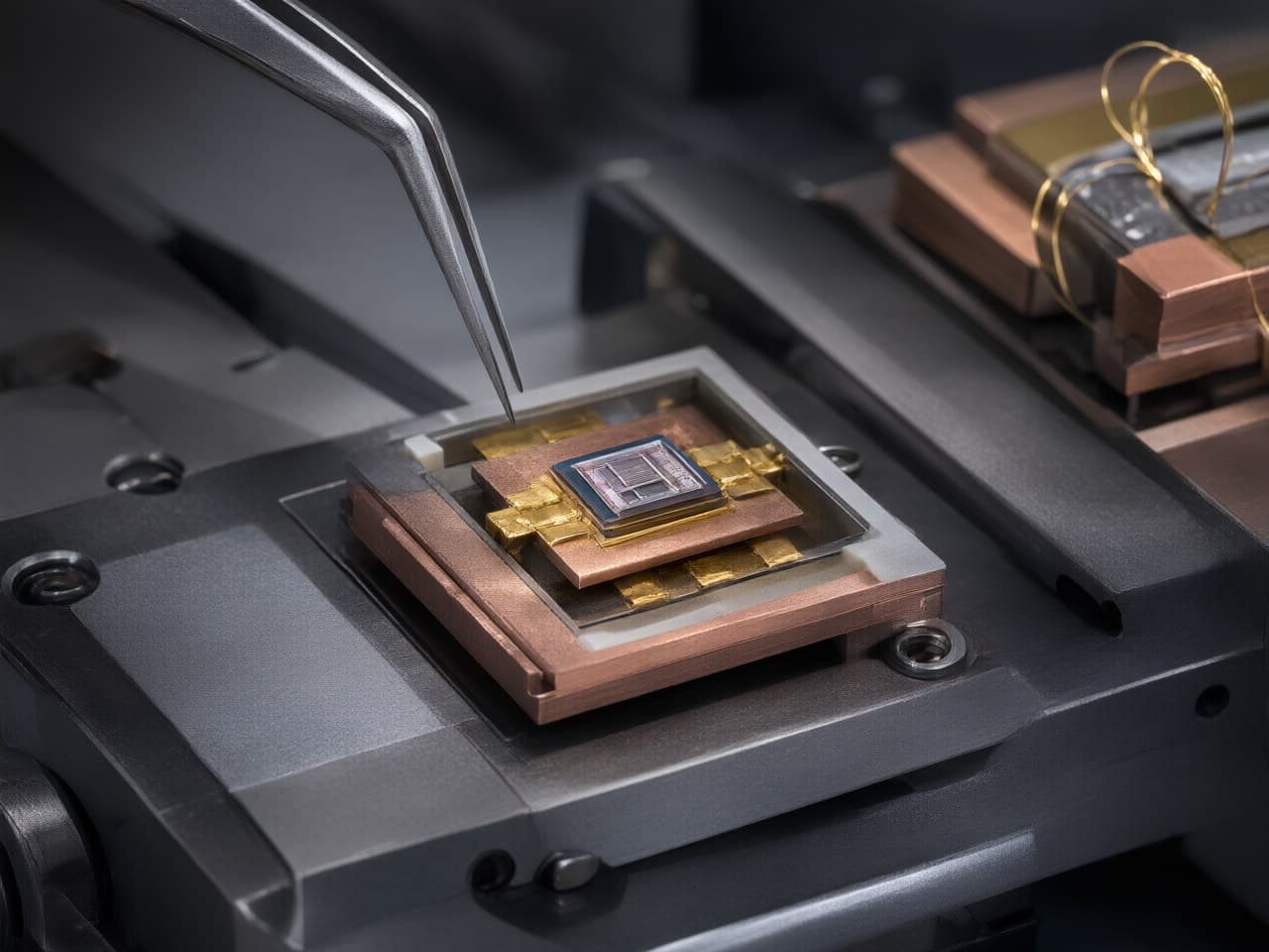
A laser submount is chosen for what it does to the die during a temperature swing, not only for how much heat it can move in a steady state. That is why tungsten copper (W–Cu) is a common conductive-submount choice for EML and DFB packages, even though pure copper conducts heat better and an aluminium nitride ceramic can match indium phosphide expansion more closely while also isolating electrically. W–Cu can keep a brittle InP or GaAs die, the specified die-attach joint, and a Kovar housing or ceramic carrier in one strain stack, without imposing the full expansion mismatch of pure copper, and it remains a metal part that can be priced at telecom volume.
Newlife - MIM supplies W–Cu, pure copper and copper-alloy carriers, submounts and thermal blocks for EML/DFB laser packaging, formed by MIM/PM near-net shape. Published capability figures for that route include a sintered density ≥8.4 g/cm³ stated for the pure-copper / copper-alloy / W–Cu MIM family, near-net micro-fins, micro-channels and cavities, and high-precision near-net-shape control at relative density ≥98% with tolerances of ±0.3%–0.5%. The absolute-density figure is discussed with the audit list below: it must not be read as the density of a dense tungsten–copper part. This article is the engineering reasoning behind the material choice, and the ways that reasoning fails when composition, density and flatness are not controlled.
EML/DFB Submounts Are a CTE Problem Before They Are a Heat-Spreading Problem
The dominant wear-out mechanism in the die-attach layer is cyclic strain, not bulk overheating of the submount. Indium phosphide is commonly reported near 4.6 ppm/°C, gallium arsenide near 5.7 ppm/°C and silicon near 2.6 ppm/°C at room temperature; all three shift with temperature, doping and orientation. Copper is commonly reported near 16–17 ppm/°C near room temperature, and the mean coefficient over a wider cycle is higher. Bond an InP die directly to a copper carrier and every on/off thermal cycle imposes a shear range on the joint that a hard solder is poorly suited to survive indefinitely.
W–Cu narrows that gap because the copper fraction is a composition variable, not a fixed property of the metal. Commercial heat-sink and contact grades sit between the tungsten-rich and copper-rich ends of the system, so CTE and conductivity move together and have to be taken from the certificate for the grade actually supplied. Specify that certified CTE band. Do not treat a weight-percent window as a material constant.
Gold–tin eutectic, the usual laser die attach, is a hard solder. Softer joints, such as indium, shed strain by creep and are a different reliability case. Neither joint type removes the need to match expansion; each only changes how the mismatch is stored.
Tungsten Copper Sits Between Pure Copper and Ceramic on the CTE–Conductivity Trade-off
No submount material wins on every axis. The comparison below is a constraint set, not a ranking.
| Route | CTE | Thermal conductivity | Electrical isolation | Near-net shape complexity | Relative cost at telecom volume (directional, not a quote) | Principal constraint |
|---|---|---|---|---|---|---|
| Pure copper (MIM/PM) | ~16–17 ppm/°C near room temperature (metals handbooks) | Highest of the metals here | No | High where the MIM/PM route can hold micro-fins, micro-channels and cavities | Low–moderate | Die-attach strain from the large CTE mismatch with InP or GaAs |
| W–Cu (MIM/PM, Cu fraction tunable) | Between tungsten and copper; grade-specific certificate | Moderate to high; rises with copper content | No | High, but limited by fill, sinter flatness and section thickness | Moderate | Copper bleed, sweating, and density or composition gradients if infiltration or sintering is not controlled |
| AlN ceramic | Near the InP band; use the ceramic certificate | Moderate | Yes | Low — typically planar metallised tiles | Moderate–high | Brittle; depends on metallisation quality; little scope for 3D features |
| AlSiC (metal-matrix composite) | Grade-dependent (set by SiC fraction); use supplier data | Moderate | No, unless a dielectric layer is added | Low–moderate | High | Finishing cost; CTE is only as good as the certified grade |
| Kovar / Alloy 42 | Low, in the semiconductor/ceramic band; heat treatment and temperature range specific | Low | No (both are metals) | Moderate | Low | Low conductivity can make the carrier the thermal bottleneck it was meant to remove |
Any row can be the right one. Only one row will satisfy die size, dissipated power, whether the submount must isolate, package CTE and price at the same time. Directional entries above are not lot values. Bind CTE, conductivity and isolation to the supplier certificate for the specific grade.
A Shear-Strain Estimate and a One-Dimensional Conduction Check Bound the Choice Before Hardware Exists
Two screening relations cover the argument that usually decides the material. They are not life models, and they are not a substitute for a temperature-cycle qualification. Evaluate them with the die size, the power and the certified CTE and conductivity already in the drawing package.
Die-attach shear strain from CTE mismatch. If the die and the submount are treated as rigid relative to a thin bond line, and the temperature change is uniform, the imposed shear strain from the centre of the attach to the edge is
γ ≈ (α_sub − α_die) · ΔT · L / (2 · t)
where α is the linear expansion coefficient, ΔT is the cycle amplitude, L is the full attach length (edge to edge), and t is the bond-line thickness. The factor of two assumes the neutral point is at mid-length. Units cancel: the result is a dimensionless strain.
Under that rigid-adherend assumption the estimate is an upper bound on joint shear, because real die and submount compliance, fillet geometry and creep all relieve some of the imposed strain. It is still the right screening comparison. Shear strain scales with mismatch, temperature swing and attach length, and it falls in the same proportion as bond-line thickness rises. Moving from a pure-copper carrier toward a W–Cu grade whose certified CTE is closer to the die therefore attacks the same term as a thicker joint, and a thicker joint costs thermal resistance. Gold–tin will store that strain; a soft solder will creep it out and may ratchet instead. The estimate does not predict cycles to failure. Models of that kind need joint-specific parameters and are not evaluated here.
One-dimensional conduction through the submount.
ΔT = P · t / (k · A)
where P is the power crossing the section, t the thickness under the die, k the through-thickness conductivity and A the area that power is assumed to cross. Units are kelvin. This is pure one-dimensional conduction. It ignores spreading, interface resistance and every other drop in the package, so it underestimates the temperature rise whenever the die is smaller than the submount and heat has to spread. It shows whether submount conduction belongs in the same conversation as the strain problem. It is not a prediction of case or junction temperature.
The conduction drop scales with power and thickness and falls with conductivity and area. On a low-dissipation DFB the conductivity difference between a suitable W–Cu grade and pure copper is often secondary to the strain problem. On a higher-power EML or a pump laser the balance can flip, and the practical answers are a thinner W–Cu section, a copper spreader beneath it, or a graded stack — checked with the real power and the certified conductivity, not with a generic ranking. Run both relations with the actual inputs before arguing about materials. They do not cover submount bow, plating adhesion, hermetic leak or optical alignment.
The Usable Design Window for a W–Cu Laser Submount Is Set by Copper Content, Bond-Line Thickness and Flatness
Four parameters carry almost all of the design freedom.
- Copper content tunes CTE and conductivity together. Specify the CTE target and the allowable band, not only a grade name. The same nominal grade can move across a lot boundary if infiltration or copper distribution is not controlled. There is no single weight-percent window that defines a good laser submount. - Thickness trades conduction drop against the flatness that can be held after sintering, and against how much joint strain the stack will impose. Telecom submounts are thin relative to the package; the acceptable thickness is the one that meets the thermal budget and the flatness callout, not a universal thickness rule. - Bond-line thickness and joint alloy are designed with the submount, not after it. Metallisation has to suit the solder and the wire-bond process. A nickel barrier with a gold finish is a common industry stack; it has to be specified and adhesion-tested on the real surface, not assumed from the base metal. - Geometric complexity. MIM/PM near-net shaping is what makes micro-fins, micro-channels and cavities practical on a small copper or W–Cu part, instead of machining them from stock. Features the tool cannot fill, or that sintering cannot hold flat, are not free complexity.
Where the Process Breaks:
Copper Bleed, Density Gradients and Shrinkage Drift
W–Cu is not a solid-solution alloy. The established industrial routes are a sintered tungsten skeleton infiltrated with copper, or a blended powder compact taken through liquid-phase sintering. Forming can be isostatic pressing, die pressing, extrusion or injection moulding, depending on shape and on who is making the part. A common way the route fails is to treat that composite as if it were a simple wrought metal.
- Copper bleed and sweating during an over-aggressive sinter or infiltrate cycle leave copper-rich surface pools and dimensional loss, and they spoil plating adhesion. The defect can remain invisible until plating. - Density and composition gradients appear when infiltration is uneven across a thin part or a long flow path. CTE then varies from point to point, and a coupon CTE can disagree with the CTE under the die. - Shrinkage drift on an injection-moulded variant shows up as flatness and coplanarity error. That becomes a die-attach void problem, not a line item on a dimensional report. - Binder residue in a copper-bearing MIM feedstock is a real risk if the debinding and sintering profile is not matched to that feedstock. Residual carbon changes wetting and can hold the part below the density the route is capable of.
Open or connected porosity is a plating and leak risk if the part sits on a hermetic boundary. Whether porosity is closed, and what the density actually is, has to be shown on the finished geometry. A relative-density figure on a process capability statement is not, by itself, a hermeticity or plating qualification.
When MIM Is the Wrong Answer for a Laser Submount
MIM is a poor fit when the geometry is essentially planar and the volume justifies a stamped or metallised ceramic tile; when the copper fraction is high enough that a near-full-density injection-moulded composite is difficult to control and a press-and-infiltrate route is more robust; when the flatness callout is tighter than sintering can hold without a finishing operation that erases the cost advantage; or when electrical isolation is mandatory and a ceramic is the compliant answer. It is also the wrong answer for a one-off build, where a machined prototype communicates the design faster than a tool. Say so in the DFM review. A supplier who will name the geometry that should not be injection moulded is more useful than one who quotes every print.
Auditable Process Evidence Matters More Than a Datasheet Number
A CTE figure on a certificate is a claim about a coupon unless the process behind it is controlled and the measurement is on the real geometry. For EML/DFB submount work, the Newlife - MIM capabilities a design engineer can put on an audit checklist are the ones published for this route:
- In-house powder engineering: self-developed ultrafine copper, iron and nickel powders (D50≤3μm) and customised MIM feedstock. That is where sintering behaviour and lot-to-lot stability start. The D50 figure is a powder size, not a feature tolerance on the submount. - Pure-copper, copper-alloy and W–Cu MIM, with a published sintered density ≥8.4 g/cm³ for that family, and near-net-formed micro-fins, micro-channels and cavities that would otherwise be machined from copper stock. Do not read ≥8.4 g/cm³ as the absolute density of a dense tungsten–copper submount. That figure sits at the copper end of the family; tungsten–copper is a much heavier composite, and a W–Cu lot has to be accepted on its own certified absolute density and CTE. The published precision figure stated on a relative basis is relative density ≥98%. - High-precision near-net-shape control at relative density ≥98%, with tolerances in the ±0.3%–0.5% band. That band is an as-sintered dimensional tolerance, not a flatness or coplanarity callout in micrometres. Flatness still has to be agreed against the die-attach void limit, and a finishing step may be required. - A quality system certified to IATF 16949, ISO 9001 and ISO 14001, with 20+ sintering furnaces, and full-chain coverage from mixing and granulation through injection, debinding, sintering and post-processing.
Those registrations show that a quality system exists. They do not replace first-article CTE, density, conductivity and plating-adhesion data on the actual submount, and they do not replace a joint-level temperature-cycle qualification.
Next Steps: Qualify the Submount Against Your Own Temperature Cycle
Move from material to a decision in five steps. First, fix the die material, the die footprint, whether the submount must isolate electrically, and the dissipated power. Second, evaluate the shear-strain and one-dimensional conduction relations above with those inputs and with certified α and k, and identify which limit binds. Third, specify a CTE band rather than a grade name, and a flatness callout tied to the die-attach void limit. Fourth, request first-article CTE, density, conductivity and plating adhesion on the actual geometry, not on a coupon. Fifth, qualify with a temperature-cycle and damp-heat test at the joint, in parallel with wavelength-drift measurement on the assembled module.
Take those measured numbers to the Newlife - MIM application engineering team. Visit http://www.newlife.cn to review the EML/DFB thermal-component range and the copper-alloy portfolio, and contact the Newlife - MIM application engineering team for a free consultation and a custom engineering solution — including a DFM review of the submount geometry, a CTE-matched W–Cu grade proposal, and a prototype plan built around the qualification cycle.
References
1. Ioffe Institute, New Semiconductor Materials archive, thermal properties of InP, GaAs and Si. http://www.ioffe.ru/SVA/NSM/ 2. CRC Handbook of Chemistry and Physics, linear thermal expansion of copper (current edition table; mean coefficients over a device temperature cycle are higher than the room-temperature value). 3. ASTM B702, Standard Specification for Copper-Tungsten Electrical Contact Materials and Electrical Contacts, ASTM International. Cited as the contact-material specification, not as a source of laser-submount class compositions. 4. Engelmaier, W., "Fatigue Life of Leadless Chip Carrier Solder Joints During Power Cycling," IEEE Transactions on Components, Hybrids, and Manufacturing Technology, vol. CHMT-6, no. 3, pp. 232–237, 1983. Cited only to mark that joint life models need their own parameters; none are evaluated in this article. 5. German, R.M., Sintering Theory and Practice, Wiley, 1996. 6. German, R.M. and Bose, A., Injection Molding of Metals and Ceramics, Metal Powder Industries Federation, 1997. 7. Newlife Materials, tungsten–copper substrate product page: http://www.newlife.cn/zh/products/tungsten-copper-substrate 8. Newlife - MIM: http://www.newlife.cn