
Overcoming the thermal barrier in next-generation AI ASICs
Published:
Republished by Newlife - MIM. All rights belong to the original publisher; see Source below.
As the demand for custom AI ASICs and HPC hits unprecedented levels, electronic design engineers are facing a severe, multi-faceted roadblock: thermal management at the semiconductor and system level.
As deep learning architectures demand higher computational density, ASICs optimised for AI are reaching unprecedented thermal power densities that challenge the traditional laws of semiconductor physics.
Conventional cooling approaches at the chassis level are no longer sufficient to mitigate the localised hotspots that degrade performance and shorten chip lifespans.
For electronic design engineers, thermal management has shifted from a post-design packaging consideration to a primary constraint dictated at the earliest stages of silicon architecture. In this feature we explore how 2.5D and 3D advanced packaging techniques, innovative thermal interface materials, and electro-thermal co-design are reshaping AI hardware to break through this looming thermal barrier.
The Silicon Hotspot Problem
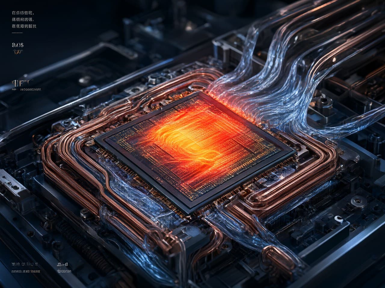
With the commercial deployment of 3nm process nodes and beyond, engineers can now pack billions of transistors into microscopic silicon footprints. However, this massive surge in transistor density has not been matched by a proportional reduction in operating voltage. The direct consequence is an extreme concentration of energy within localised areas of the die.
Matrix multiplication units (MACs) and tensor accelerators, operating under continuous training and inference workloads, run at peak capacity simultaneously, driving local heat flux densities well beyond 1000 W/cm².
This non-uniform power distribution creates severe micro-architectural anomalies known as silicon hotspots. In these specific zones, temperatures spike drastically compared to adjacent, less active areas of the chip, such as memory interfaces or I/O blocks. These extreme thermal gradients induce harsh mechanical stresses caused by coefficient of thermal expansion (CTE) mismatches between the silicon die, the microbumps, and the substrate.
Left unchecked, this localised thermomechanical stress triggers microcracking and structural fatigue, severely compromising the long-term reliability of mission-critical AI hardware.
In this hyper-dense environment, legacy air cooling systems - such as copper heatsinks combined with high-RPM fans - are completely obsolete. Even modern direct-to-chip liquid cooling solutions, which have become standard in enterprise data centres, are hitting a physical wall. Heat simply cannot escape fast enough from the transistor junction to the cooling fluid.
Consequently, on-chip management algorithms instantly trigger thermal throttling, forcing clock frequencies down to protect the silicon and crippling the raw processing throughput these 3nm chips were built to deliver.
Advanced Packaging Solutions
To break through the thermal restriction of 3nm nodes, the semiconductor industry is moving away from monolithic single-die designs toward advanced packaging methodologies. Digital architectures utilising 2.5D integration (such as TSMC’s CoWoS) and 3D stacking (where compute chiplets are layered vertically over a base die) provide massive interconnect density.
However, vertical integration introduces a critical three-dimensional thermal challenge: heat generated by upper-layer dies must propagate through additional silicon layers, thin-film adhesives, and through-silicon vias (TSVs) before reaching the heatsink. To counter this, engineers are adopting strict electro-thermal co-design strategies at the architectural phase, strategically interleaving high-power compute blocks with passive or structural chiplets that act as embedded thermal conduits to evenly distribute heat across the vertical column.
In parallel, one of the largest sources of latent heat generation in legacy AI accelerators stems from the high-speed electrical I/O interfaces required to bridge the processor with HBM stacks and external network switches.
Traditional copper-based transceivers dissipate substantial thermal energy due to ohmic losses when driving signals at ultra-high baud rates. The deployment of Co-Packaged Optics (CPO) mitigates this issue at the foundation by replacing long-reach electrical links with silicon photonics engines mounted directly onto the same package substrate.
By transitioning electrons to photons for high-throughput data routing, CPO slashes I/O power consumption by up to 50% compared to discrete pluggable optical modules or legacy copper topologies. This drastic drop in power demand not only optimises overall system efficiency but effectively eliminates the dense, peripheral thermal boundaries that typically surround the processor core.
As a result, swapping copper traces for optical waveguides frees up vital thermal headroom within the package layout, allowing external cooling mechanisms to focus their extraction capabilities exclusively on the high-performance logic engines.
Innovative Thermal Materials
When physical limits prevent heat from escaping rapidly from the silicon, materials science becomes the last line of defence for AI hardware designers. Legacy polymer-based Thermal Interface Materials (TIMs) and silicone greases can no longer handle the extreme demands of 3nm dies; their low thermal conductivity (typically below 5 W/m·K) creates an unacceptable thermal resistance barrier.
To eliminate this constraint, the industry is transitioning toward metallic TIMs, specifically liquid metal alloys (such as gallium-indium) and preformed indium foils. These compounds offer a thermal conductivity well exceeding 60 W/m·K and achieve a near-perfect microscopic compliance between the silicon surface and the heatsink, effectively eliminating the insulating air micro-voids that degrade heat transfer.
At the upper boundary of the package, conventional nickel-plated copper Integrated Heat Spreaders (IHS) are being optimized or replaced by highly oriented graphene films. Graphene possesses an exceptional in-plane thermal conductivity that tops 1500 W/m·K, outperforming copper by more than three times.
By integrating graphene layers directly over the ASIC's localised hotspots, heat is not just driven vertically toward the cooling solution but is spread laterally across the component's surface at ultra-high speeds.
This multidirectional dissipation flattens severe localised temperature spikes by tens of degrees Celsius, transforming a dangerous, uneven thermal profile into a homogeneous load that is far easier to evacuate via liquid or phase-change cooling systems.
Design Best Practices
Successfully overcoming the 3nm thermal barrier demands a complete shift away from sequential design pipelines. Systems engineers can no longer relegate thermal management to the final validation stages; they must enforce a thermal-mechanical-electrical co-design methodology from the hardware's initial conceptualization.
This shift requires simulating thermal behaviour in parallel with high-speed signal routing using advanced Finite Element Analysis (FEA) and Computational Fluid Dynamics (CFD) tools. By mapping expected power profiles early on, engineers can predict thermomechanical stresses arising from CTE mismatches and adjust the layout of TSVs and microbumps before committing to wafer fabrication.
Furthermore, designers must deploy intelligent power architectures and active board-level management. This is achieved by embedding dense networks of on-chip thermal diodes tied to fast-response digital Power Management ICs (PMICs).
Instead of relying on a global emergency shutdown, engineers should program granular, dynamic throttling algorithms. By selectively scaling down clock frequencies only within specific logic blocks hitting critical thresholds, the overall throughput of the AI ASIC is preserved.
Finally, the selection of low-profile substrates and the strategic integration of heavy copper ground planes within the printed circuit board (PCB) layout should be utilised to turn the motherboard itself into a highly effective secondary heat sink.
Conclusion
As 3nm process nodes and three-dimensional packaging topologies push semiconductors to their absolute physical boundaries, innovation in thermal management has emerged as the definitive backbone of modern hardware performance. Breaking through the thermal barrier demands a seamless integration of materials science, advanced packaging, and rigorous front-end architectural co-design. Electronic design engineers who adopt these holistic methodologies today - moving away from isolated, legacy cooling patches - will define the true operational ceiling for the next generation of intelligent computing.
Source
- newelectronics.co.uk (2026-08-24) - Original article: Overcoming the thermal barrier in next-generation AI ASICs - https://www.newelectronics.co.uk/content/features/overcoming-the-thermal-barrier-in-next-generation-ai-asics