
What New Requirements Does Co-Packaged Optics (CPO) Place on Thermal Components? Materials and Structural Responses
Published:
What New Requirements Does Co-Packaged Optics (CPO) Place on Thermal Components? Materials and Structural Responses
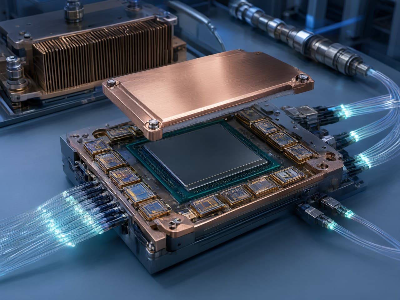
Co-packaged optics (CPO) moves optical engines from the faceplate onto the same package substrate as the switch or accelerator ASIC. The goal is shorter electrical paths and lower interconnect power. The cost is a harder thermal problem. A high-power ASIC now shares that substrate with photonic and laser components that are more temperature-sensitive than the SerDes circuitry previously kept at the faceplate. Thermal parts that were once simple lids or pluggable-module spreaders now have to work as precision, multi-functional, CTE-aware structures.
This article looks at how that trend changes requirements for heat spreaders, lids, and submounts. It then covers which materials and forming routes respond best, and where metal injection molding (MIM) fits and where it does not.
Co-packaged optics thermal management turns heat spreaders into precision structural parts
In CPO, the thermal part is no longer a commodity block of copper. It has to control heat flux, flatness, and thermo-mechanical stress at the same time. Four shifts drive this change:
- Heat-flux density and proximity. The ASIC and optical engines share a substrate and often a lid or cold plate. Heat has to spread laterally so that hotspots do not raise the temperature of nearby photonic zones. That favors high-conductivity copper close to the die. - CTE mismatch at multiple interfaces. Silicon photonic chips, ceramic or organic substrates, and laser submounts each expand differently. A spreader that is excellent thermally but badly mismatched in CTE can warp the assembly or load solder and adhesive joints during thermal cycling. - Geometric complexity. Thermal paths in CPO packages tend to need steps, pockets, local pedestals, fiber-routing reliefs, and sometimes micro-fins or micro-channels. Machining these features from solid stock in volume is expensive. - Surface and joining readiness. Parts must accept the specified electroplating, soldering, wire bonding, or brazing without blistering or outgassing. Those finishes are drawing requirements, not properties implied by the alloy name alone.
For procurement, the result is a shift from buying “a thermal material” to qualifying a supplier that can co-optimize material, geometry, and finish.
Side-by-side comparison shows which material and forming route fits each CPO thermal part
For CPO thermal parts, the usual split is pure copper where conductivity dominates, and tungsten copper (W-Cu) where CTE matching dominates. Each is formed by the route that matches the geometry and volume.
| Route / material | Strengths for CPO | Limitations | Typical fit |
|---|---|---|---|
| CNC from wrought copper | Highest design freedom at low volume; conductivity of wrought copper | Material removal, cycle time, and scrap rise as pockets, fins, and steps multiply; wrought copper CTE is fixed | Prototypes and simple flat lids |
| Stamping / skiving copper | Low piece cost at volume for flat or simple finned shapes | Limited to shapes the forming tools can make; not a route to multi-level pockets, steps, and enclosed channels | Large simple lids and standard fin stacks |
| Press-and-sinter or infiltrated W-Cu, plus machining | CTE closer to ceramics and semiconductors than pure copper; good stiffness | Complex shapes usually need more machining than a near-net route; W-Cu is denser and heavier than copper | Simpler laser submounts and housings |
| MIM/PM near-net copper or W-Cu, with machining only on critical faces | Micro-fins, thin walls, pockets, and steps formed near net; W-Cu available when CTE matching is required; machining limited to datums | Tooling cost needs volume; section size is limited by debinding and sintering | Compact optical-engine spreaders, chip bases, and similar volume parts |
Newlife - MIM applies the hybrid route in the last row to pure copper, copper alloy, and tungsten-copper MIM. Micro-fins, micro-channels, and cavities are formed near net, so those features do not have to be machined entirely from solid copper. Post-processing is part of the same process chain and can include machining of faces the drawing holds as datums. Published precision control for this near-net route is relative density ≥ 98% and dimensional tolerances of ±0.3% to ±0.5%. On optical transceiver heat spreaders, laser diode heat sinks, and pump laser diode coolers, sintering to a relative density of ≥ 98% keeps mechanical properties close to wrought material. Those figures describe density and size control. They do not, by themselves, establish wrought-equivalent conductivity or a qualified plating stack. Conductivity, flatness, and joining still have to be confirmed on the part and on the finish the package actually uses.
Two simple models show why material choice and geometry decide CPO thermal performance
Path length, conductivity, area, and CTE mismatch can be ranked early with two textbook relations. Use them to avoid a late geometry change, then confirm with measurement or FEA.
1. One-dimensional conduction resistance:
R_th = t / (k · A)
Here t is the conduction path length, k is thermal conductivity, and A is cross-sectional area. The relation is steady, one-dimensional, and constant-k. It ignores side loss, spreading resistance, and interface resistance. Dimensionally, t/(k·A) is temperature difference per unit heat flow.
What it means for design and purchasing: Within those assumptions, halving the path thickness or doubling the effective area changes R_th as much as doubling conductivity. In CPO, the lid and spreader sit between the die, the TIM, and the cold plate. Local pedestals that shorten t over the hotspot, or fins that enlarge A, are often stronger levers than a more exotic alloy. A thinner section can raise spreading resistance and can be harder to debind, so the geometric lever has a floor. Near-net forming is the volume route that makes pedestals, pockets, and fins practical when machining them from solid copper is a poor fit. Rank options with this relation, then confirm with FEA and a thermal mock-up.
2. Thermal mismatch strain between bonded layers:
Δε ≈ (α₁ − α₂) · ΔT
Here α₁ and α₂ are the coefficients of thermal expansion of the two bonded materials, and ΔT is the temperature swing. Δε is a dimensionless free (unconstrained) mismatch strain. It is not the stress in the joint. Stress and warpage also depend on modulus, thickness ratio, and how the stack is constrained. The single ΔT assumes both materials see the same temperature change. In a powered CPO package they often do not.
What it means for design and purchasing: Free mismatch strain scales with the CTE gap and with the temperature swing used in the estimate. Reflow, power cycling, and ambient change can all be large, so a moderate CTE gap is worth checking before the stack is frozen. This is why W-Cu is considered where a spreader bonds directly to a chip or a ceramic. Composition can move its CTE toward the mating material, at the cost of conductivity relative to pure copper. Pure copper remains the conductivity-first choice where a compliant TIM decouples the joint. Do not treat Δε as a fatigue life or a warpage number; those need the stiffness of the actual stack.
A process scaling note, not a third thermal model, matters for MIM. The cavity is oversized for sintering shrinkage:
cavity dimension ≈ part dimension / (1 − linear shrinkage)
Linear shrinkage here is the fractional contraction from the cavity (or green) dimension to the sintered dimension, not an expansion factor defined on the finished part. The relation assumes isotropic shrinkage. Shrinkage consistency, not only the nominal value, decides whether a flatness-critical face can be left as-sintered or must be machined.
MIM copper and tungsten-copper parts fit a limited CPO design window
MIM pays off when a CPO thermal part is small, three-dimensional, and needed in volume. Machine or lap only the faces that set flatness and the thermal interface.
Use these guidelines when drafting a CPO spreader or submount for MIM/PM:
- Size and mass: Favor compact parts typical of optical engines, laser submounts, and chip bases. Large monolithic lids are usually better stamped or machined. - Wall uniformity: Keep sections as uniform as practical. Transition thick pedestals into thin fins gradually, and core out heavy bosses, so debinding and shrinkage are not driven by abrupt thickness changes. - Datum strategy: Specify which faces contact the die, TIM, or cold plate. Allow machining or lapping stock only there. Leave fins, pockets, and reliefs as-sintered unless a datum says otherwise. - Tolerance expectations: Plan as-sintered dimensions against Newlife - MIM’s published tolerance band of ±0.3% to ±0.5% of dimension. Tighter flatness belongs on a machined or lapped face. Do not treat that band as a universal MIM standard for every supplier. - Finish and joining: Call out the plating stack (for example Ni/Au or Ni/Ag), the solder or braze process, and the bond-pad areas on the drawing. Surface preparation depends on them. Naming an example stack does not mean that stack is already qualified on a given part. - Material split: Use pure copper where conductivity dominates. Use W-Cu where the part bonds rigidly to a semiconductor or a ceramic. Copper alloy is part of the same MIM set, but it is not a substitute for that split unless the alloy’s conductivity and CTE have been checked for the joint. Newlife - MIM’s relevant portfolio for this choice is pure copper, copper alloy, and tungsten-copper MIM, not a named laser-module catalog recipe.
Process risks define when MIM is the wrong choice for CPO thermal parts
MIM is not automatically better. Thick sections, very low volumes, and flatness the sintered state cannot hold are reasons to choose another route or a hybrid.
Key process risks to discuss with any supplier, including Newlife - MIM:
- Debinding cracks or blisters in thick or abruptly changing sections, where binder cannot leave uniformly. - Distortion from uneven walls, which shows up as warpage on the faces CPO needs flat. - Residual carbon or oxygen from binder and atmosphere. On copper, either can lower conductivity and interfere with plating. Density does not prove the interstitial chemistry. Ask how it is controlled and how conductivity and plate adhesion are verified on the finished part. - Shrinkage scatter between lots, which consumes the tolerance budget before any machining stock is applied.
A thermal boundary sits beside these process risks. A copper or W-Cu spreader can lower conduction resistance and can reduce free mismatch strain. It does not remove TIM or cold-plate resistance, and it does not replace temperature control of a laser or modulator.
MIM is usually the wrong fit when:
- annual volume cannot amortize tooling, - the part is a large, simple flat plate, - every surface needs lapped flatness anyway, so near-net forming saves little machining, - the design is still changing from week to week — prototype by CNC, and move to MIM only after the geometry freezes, or - the thermal budget assumes wrought-copper conductivity and the shape does not need near-net 3D features. Sintered conductivity has to be measured. Relative density does not prove it.
Newlife - MIM can show powder, density, and process-control evidence for CPO thermal parts
Judge a MIM thermal supplier on powder, density, and process control that can be checked, not on an unstated product recipe. For CPO spreaders and submounts, Newlife - MIM’s relevant published capability is:
- Copper and W-Cu near-net forming. Pure copper, copper alloy, and tungsten-copper MIM are specified at a sintered density of ≥ 8.4 g/cm³. Micro-fins, micro-channels, and cavities are formed near net to replace costly copper machining. That is the geometric overlap with compact CPO spreaders, submounts, and chip bases. It is not a claim that a catalog part is already qualified to a named photonic device, or that every part is plated, vacuum-brazed, or lapped to a stated stack. - How to read the two density figures. Sintered density of ≥ 8.4 g/cm³ is the published minimum across pure copper, copper alloy, and tungsten-copper MIM. It is not the density of a specific W-Cu grade. Relative density ≥ 98% is a separate published control. On optical transceiver heat spreaders, laser diode heat sinks, and pump laser diode coolers, sintering to a relative density of ≥ 98% keeps mechanical properties close to wrought material. Absolute density cannot be converted to relative density without the theoretical density of the alloy actually molded, so the two figures must not be treated as one measurement, and neither figure is a conductivity specification. - In-house powder and feedstock. Ultra-fine copper, iron, and nickel powders with D50 ≤ 3 μm are developed in-house, and MIM feedstocks are customized. For the copper and tungsten-copper thermal parts in this article, ask how the copper powder and the feedstock lot are tied to the finished part. The D50 figure is not a tungsten-powder specification. - Process chain. Mixing, granulation, injection, debinding, sintering, and post-processing are covered in-house. That is the scope to audit when asking about binder removal, atmosphere, and finishing. - Precision control. Published control for this near-net route is relative density ≥ 98% and tolerances of ±0.3% to ±0.5%. Request density data, dimensional reports, and Cpk on the critical features of the part under qualification. - Joint development. OEM/ODM co-development and rapid prototyping for complex micro-structures are the practical way to freeze CPO geometry before tooling.
Engineering and sourcing teams should fix the material split and datums before choosing a route
Settle the material split and the datum strategy first. Forming-route economics follow from that, not the other way around.
1. Map hotspots and temperature-sensitive optical zones on the package layout. 2. Decide where conductivity dominates (copper) and where CTE matching dominates (W-Cu). 3. Rank geometry with R_th = t/(k·A), and check free mismatch strain with Δε ≈ (α₁ − α₂)·ΔT. Confirm both with FEA before tooling. 4. Mark the faces that must be machined or lapped, and leave the rest near net. 5. Define plating, solder, braze, and bonding on the drawing. Do not infer them from density or from the alloy family. 6. Ask suppliers for density, dimensional Cpk, conductivity if the thermal budget needs it, and powder-lot traceability. 7. Contact Newlife - MIM for engineering support on this class of part. Visit http://www.newlife.cn to request a consultation, a DFM review of the CPO spreader or submount, and a copper or W-Cu MIM approach built around that package.
References
1. German, R. M., & Bose, A. Injection Molding of Metals and Ceramics. Metal Powder Industries Federation, 1997. 2. Heaney, D. F. (Ed.). Handbook of Metal Injection Molding. Woodhead Publishing. 3. Incropera, F. P., DeWitt, D. P., Bergman, T. L., & Lavine, A. S. Fundamentals of Heat and Mass Transfer. Wiley. 4. MPIF Standard 35, Materials Standards for Metal Injection Molded Parts. Metal Powder Industries Federation. 5. Optical Internetworking Forum (OIF). Co-Packaging Framework documentation. oiforum.com. Architecture context only; no thermal number in this article is taken from OIF. 6. Newlife - MIM. Published process capability for pure copper, copper-alloy, and tungsten-copper MIM (sintered density, relative density, dimensional tolerance, in-house Cu/Fe/Ni powder size, process chain, and OEM/ODM development). http://www.newlife.cn