
How to Choose Materials for 800G/1.6T Optical Module Heat Spreaders? Conductivity, CTE and Forming Route for Copper, W-Cu and AlSiC
Published:
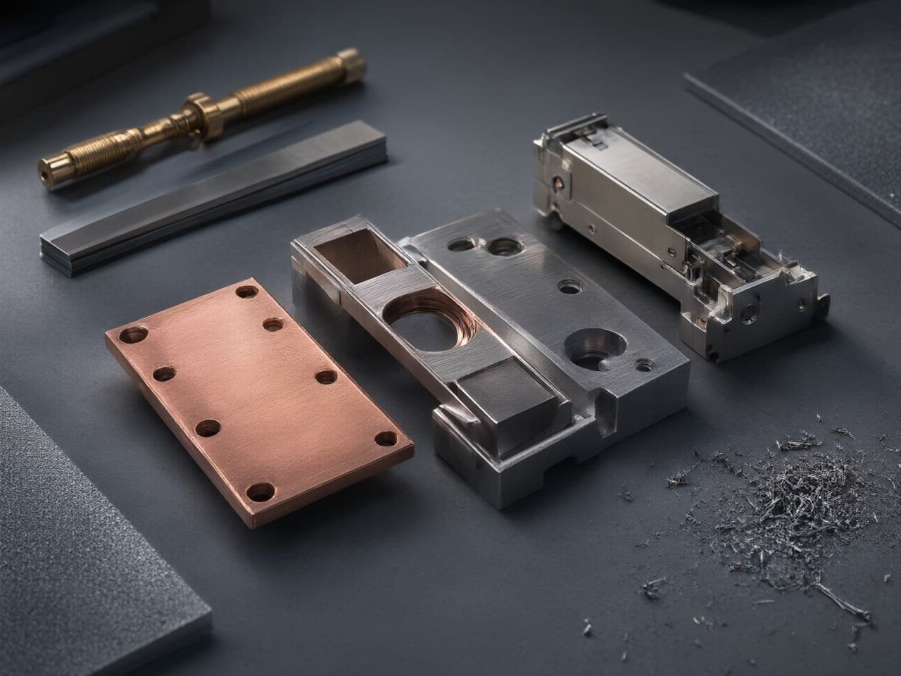
How to Choose Materials for 800G/1.6T Optical Module Heat Spreaders? Conductivity, CTE and Forming Route for Copper, W-Cu and AlSiC
The material decision for a pluggable optical-module heat spreader is set by three constraints, not one: thermal conductivity, coefficient of thermal expansion (CTE) against the surfaces the spreader actually touches, and whether the MSA envelope can be filled with a geometry the chosen process can form. Copper leads on conductivity, W-Cu can be tuned for CTE, and AlSiC leads on mass and specific stiffness. For an 800G QSFP-DD or OSFP lid, envelope and cost per part often favor copper or W-Cu once the shape is no longer a flat plate — and near-net-shape forming is then worth pricing against machining. Which alloy, and how thick, still has to be closed in a spreading model, not from conductivity alone. The cases where that comparison does not favor MIM are set out below.
The 800G-to-1.6T Transition Makes Heat-Spreader Material a Cost and Manufacturability Decision
As per-lane rates move from 800G-class modules toward 1.6T, module power tends to rise with them, and the heat spreader stops being only a lid. The module envelope stays fixed by the MSA, so the designer cannot add volume — only redistribute it. That leaves four levers: material conductivity, spreader thickness, spreading geometry (fins, pedestals, cavities), and the interfaces to the die and to the cage.
Because three of those four levers are geometry or interface, the material choice is also a manufacturing choice. A flat copper plate is a stamping or a milled billet. A W-Cu spreader with a pedestal, a stepped flange and micro-fins is a different cutting problem: tungsten-bearing material is hard and abrasive, so tool wear and cycle time push machined W-Cu cost up quickly. That is the regime in which powder metallurgy and metal injection molding (PM/MIM) near-net-shape forming is worth pricing against machining. AlSiC sits outside that trade. It is not a MIM material family; it is produced by infiltration of a SiC preform or a related composite route, and it is a different supply chain.
Copper, W-Cu and AlSiC Split the Job by Conductivity, CTE Match and Forming Route
The table uses typical published handbook bands for dense grades. Conductivity, CTE and density of W-Cu move together with composition; a grade does not sit at the favorable end of all three columns at once. Exact values depend on grade, purity, process and, for W-Cu, the tungsten-to-copper ratio. Freeze a thermal budget only against the specific supplier datasheet.
| Material family | Typical thermal conductivity (W/m·K) | Typical CTE (ppm/K) | Density (g/cm³) | Practical forming route | Where it earns its place | Where it hurts |
|---|---|---|---|---|---|---|
| Wrought pure copper (C11000-type) | ~380–400 | ~17 | ~8.9 | Rolled, stamped or milled | Highest conductivity of the three, low raw-material cost, straightforward plating and soldering | CTE well above ceramic and silicon; soft, so flatness is a design and finishing problem |
| W-Cu composite (common ~50–90 wt% W grades) | ~170–310, rising as the copper fraction rises | ~6.5–12.5, falling as the tungsten fraction rises | ~12–17, rising with tungsten fraction | Infiltrated or sintered PM; PM/MIM near-net-shape plus precision CNC on critical faces | CTE can be tuned toward alumina, BeO-class ceramics and some compound-semiconductor packages; stiff relative to copper | Conductivity below wrought copper; high density; expensive to machine — the reason near-net-shape is priced |
| AlSiC (SiC-reinforced aluminum, packaging grades) | ~160–200 | ~6.5–9 | ~3.0 | SiC-preform infiltration (near-net-shape is part of the route), then finishing and plating | Low mass, high specific stiffness, CTE tunable; used where lid mass matters | Conductivity below copper and overlapping only the low end of W-Cu; not a MIM family — different supply chain and design rules |
MIM copper is not the wrought row. Sintered density, oxygen and residual carbon move thermal conductivity off the C11000 band. Do not insert ~380–400 W/m·K into a MIM copper budget unless the sintered grade’s measured conductivity is actually there. Newlife - MIM’s published density floor for copper, copper-alloy and W-Cu MIM is given in the process section below; it is not a conductivity specification and it is not the handbook density of a W-Cu grade.
| Decision axis | Copper plate + CNC | W-Cu or copper via PM/MIM near-net-shape | AlSiC via infiltration |
|---|---|---|---|
| Tooling / NRE | Low on simple plates | Moderate; amortized over volume | Preform tooling; program-specific |
| Cost as geometry gets complex | Rises with each machined feature | Added fins, pedestals and cavities are formed, then critical faces are finished | Preform can carry complexity; finishing SiC-bearing surfaces is abrasive and slow |
| Cost as volume rises | Machining cost per part stays material-dominated | Falls as tooling amortizes | Follows preform-tooling amortization, not a MIM curve |
| Where the route fits | Prototypes and simple shapes | Mid to high volume, complex copper or W-Cu shapes | When mass or a composite CTE is the driver and the part is sourced on a composite route |
A One-Dimensional Conduction Term Compares Thickness and Conductivity; Spreading and Interfaces Still Dominate
A one-dimensional conduction estimate is a fast screen before anyone commits to a CAD model. It is not a thickness optimizer for a lid.
R_cond = t / (k · A)
with t, k and A in consistent SI units (m, W/m·K, m²), so R_cond is in K/W. Here t is the thickness along the heat path, k is thermal conductivity, and A is the area that actually carries a uniform flux. Under those assumptions only, the term scales with t and with 1/k. Doubling thickness doubles this term. It does not double the thermal resistance of a heat spreader.
Two mis-readings of A are common. If A is the full lid footprint while the source is a small die, the formula understates resistance because it ignores constriction. If A is the source area, the formula ignores the lateral spread the larger plate provides and makes extra thickness look purely harmful. Use the expression as the through-thickness term only.
Because that term scales as 1/k, moving from an AlSiC packaging grade in the table band (~160–200 W/m·K) to wrought copper (~380–400 W/m·K), at the same thickness and the same A, changes the one-dimensional term by a factor of about two. That factor is not a part-mass ratio — the densities in the table differ by about a factor of three — and it is not a spreading-resistance ratio. It also does not describe MIM copper unless measured k of the sintered grade is in the wrought band. A lower-k material is not automatically a cheaper part: it can force a thicker section, a larger footprint, or more finishing.
The second relationship is only a bracket on dense two-phase W-Cu, and only if f_W and f_Cu are volume fractions that sum to 1:
k_eff(upper) = f_W · k_W + f_Cu · k_Cu
1/k_eff(lower) = f_W / k_W + f_Cu / k_Cu
These are the parallel (upper) and series (lower) bounds. They assume constant constituent conductivities, no interfacial resistance and no porosity. Commercial W:Cu callouts are usually weight percent; tungsten and copper densities differ enough that weight percent must not be substituted for f. Residual porosity is a third phase and can put conductivity below the two-phase series bound, so an as-sintered part is not guaranteed to lie inside the bracket. This guide does not evaluate the bounds for a chosen grade — no composition has been selected, and no constituent k is inserted here.
The engineering point the bounds do support is already visible in the table: CTE match is bought with thermal conductivity. Raising tungsten content pulls CTE down and pulls k down with it. No grade maximizes both. Choose the ratio against a stated CTE target — the ceramic, die attach or package the spreader is bonded to — not against a round composition.
Both expressions omit spreading resistance, which appears when a small heat source sits on a much larger plate. In that regime, added thickness reduces spreading resistance only while the spreading term still dominates; after that, extra thickness adds mass and cost with little thermal return. Footprint and source size belong in the early model with the alloy. Thickness is chosen from a spreading calculation or a measurement, not by minimizing t/(k·A) alone.
Interface resistance at the die attach and at the TIM is often in the same order as, or larger than, the spreader’s own one-dimensional term. That is a budgeting caution, not a measured split for every module. Specifying a low-CTE composite while leaving the interface unspecified still misallocates attention: close the interfaces in the same pass as the alloy. Junction-to-case targets, where they are used, should be stated in the same sense as the JESD51-type package metrics the program already uses — this article does not compute one.
The Design Window Where MIM Heat Spreaders Beat Machined Copper
Near-net-shape powder routes pay off inside a specific envelope: complex copper or W-Cu geometry, volume enough to amortize a tool, and tolerances that match what sintering holds versus what finishing must hold.
Newlife - MIM’s published process figures for that comparison are: relative density ≥98%, tolerances of ±0.3%–0.5%, and, for copper, copper-alloy and W-Cu MIM, a sintered-density floor of ≥8.4 g/cm³, with micro-fins, micro-channels and cavities formed near-net-shape rather than cut, plus precision CNC on critical faces. Those figures are the process window a heat-spreader DFM review is checked against. They are not a measured conductivity, and ≥8.4 g/cm³ is not the density to type into the thermal table for a W-Cu grade.
For a design engineer the usable rule is: put complexity into the molded geometry, and put tolerance-critical faces onto the finishing operation. A pedestal, a stepped flange, a fin array, a cavity or a screw boss is formed rather than fully machined. Features that must hold better than the ±0.3%–0.5% window — percent of the dimension, not an absolute millimetre band — should be planned as post-sinter finishing from the first drawing, not discovered at first article. Lid flatness is usually one of those features.
Where MIM Heat Spreaders Are the Wrong Tool:
Cracks, Uneven Walls, Atmosphere and Shrinkage Scatter
MIM is not the right route for every spreader. The limits below are general MIM practice, not a claim of measured scrap on a named module.
Green and brown parts are fragile before sintering. Sharp jumps between thick and thin sections, knife-edge rims and deep isolated pockets are where debinding and sintering cracks start. Non-uniform wall thickness drives differential shrinkage, which shows up as warpage on the face that must be flat. For copper-bearing feedstock, carbon and oxygen through debinding and sintering have to be shown on the production furnace; a lab coupon does not stand in for that. Because the published tolerance is a percentage, shrinkage scatter grows with part size: a large thin spreader is harder to hold than a small thick one.
Do not use MIM when:
- The part is essentially a flat plate. With no fins, pedestals or cavities, rolled copper sheet or an extruded profile plus machining is the simpler buy. Molding a plate adds a tool and no geometric benefit. - Annual volume cannot carry the tool. Below that floor, CNC from copper bar can be cheaper even with worse material utilization. No universal volume cutoff is stated here; price it on the drawing. - The material must be AlSiC. AlSiC is not a MIM material. If mass or a composite CTE drives the choice outside copper, W-Cu and the other PM alloys Newlife - MIM actually runs, that is a different supply chain. Decide that at concept review, not after a MIM DFM cycle. - The aspect ratio is past what filling and ejection will hold. Deep, narrow micro-channels can be formed only inside a DFM limit. Bring the drawing to that review before treating a channel as moldable. No universal aspect-ratio number is claimed here.
Process Figures Newlife - MIM Can Put Against a Heat-Spreader Drawing
The figures below are published process capability, checkable in a quality-file review. They are not marketing substitutes for a grade datasheet.
- Powder and feedstock under one roof. In-house ultrafine copper, iron and nickel powder and custom MIM feedstock with D50 ≤ 3 μm. Feedstock control is a primary driver of dimensional repeatability in MIM; in-house powder is how that input is held. - Full-chain MIM/PM coverage — mixing, granulation, injection, debinding, sintering and post-processing — so the shrinkage data and the tool sit in the same process, not across unrelated vendors. - Copper, copper-alloy and W-Cu MIM with a published sintered-density floor of ≥8.4 g/cm³, and micro-fins, micro-channels and cavities formed near-net-shape where the alternative is machining them from copper. - High-precision near-net-shape control: relative density ≥98% and tolerances of ±0.3%–0.5%. Treat both as the published window, and plan inspection on the features the drawing actually controls. - Quality-system certificates: IATF 16949, ISO 9001 and ISO 14001. These are company system certifications, not a claim that a given heat spreader carries an optical-module or automotive product qualification.
For an 800G or 1.6T stack-up, engage at the engineering stage — power map, CTE targets and fin geometry — so material and DFM choices are made against those process figures rather than against assumptions carried over from the previous generation.
Send the Thermal Stack-Up to Newlife - MIM for a No-Cost DFM and Material Review
Before a heat-spreader drawing is released, assemble: the target junction-to-case resistance and the power map; the CTE of the die, ceramic or package the spreader bonds to; the MSA envelope and keep-out zones; annual and peak volumes; flatness and tolerance callouts; surface finish and plating requirements; and the intended attach method — solder, thermal adhesive or other bond.
Then go to http://www.newlife.cn and contact the Newlife - MIM team for a no-cost consultation and engineering review. Send the drawing and the thermal budget. The team replies with a material recommendation inside the alloys it actually runs — copper, W-Cu, or another PM alloy in that qualified set — a composition tied to the stated CTE target, a near-net-shape split that forms the complex features and finishes the tight faces, and a DFM review before tooling is cut. That is the point in the program where a material change is still inexpensive.
References
1. Incropera, F. P., DeWitt, D. P., Bergman, T. L., Lavine, A. S., Fundamentals of Heat and Mass Transfer, Wiley. (One-dimensional conduction and spreading as phenomena; no module measurement is taken from this source.) 2. ASM International, ASM Handbook, Volume 2: Properties and Selection — Nonferrous Alloys and Special-Purpose Materials. (Handbook context for copper and related nonferrous properties.) 3. Copper Development Association, technical resources on copper and copper alloy properties (copper.org). (Wrought copper conductivity, CTE and density band.) 4. CPS Technologies, AlSiC material datasheets and application notes. (AlSiC packaging-grade band; a named grade still overrides the table.) 5. German, R. M., Powder Injection Molding, Metal Powder Industries Federation. (General MIM defect and DFM practice used in the boundary section.) 6. JEDEC, JESD51 series — thermal measurement and modelling of semiconductor packages. (Context for how junction-to-case metrics are defined; not applied numerically here.) 7. QSFP-DD MSA and OSFP MSA published specifications (public MSA documents). (Envelope is fixed by the MSA; no MSA dimension is extracted in this article.) 8. Newlife - MIM published process figures as used above — http://www.newlife.cn. (Source for D50 ≤ 3 μm, sintered density ≥8.4 g/cm³, relative density ≥98%, tolerance ±0.3%–0.5%, and the stated quality-system certificates.)