
How to Choose Between Tungsten-Copper (W-Cu) and Pure Copper Heat Sink Substrates: The Matching Logic of Thermal Conductivity and CTE
Published:
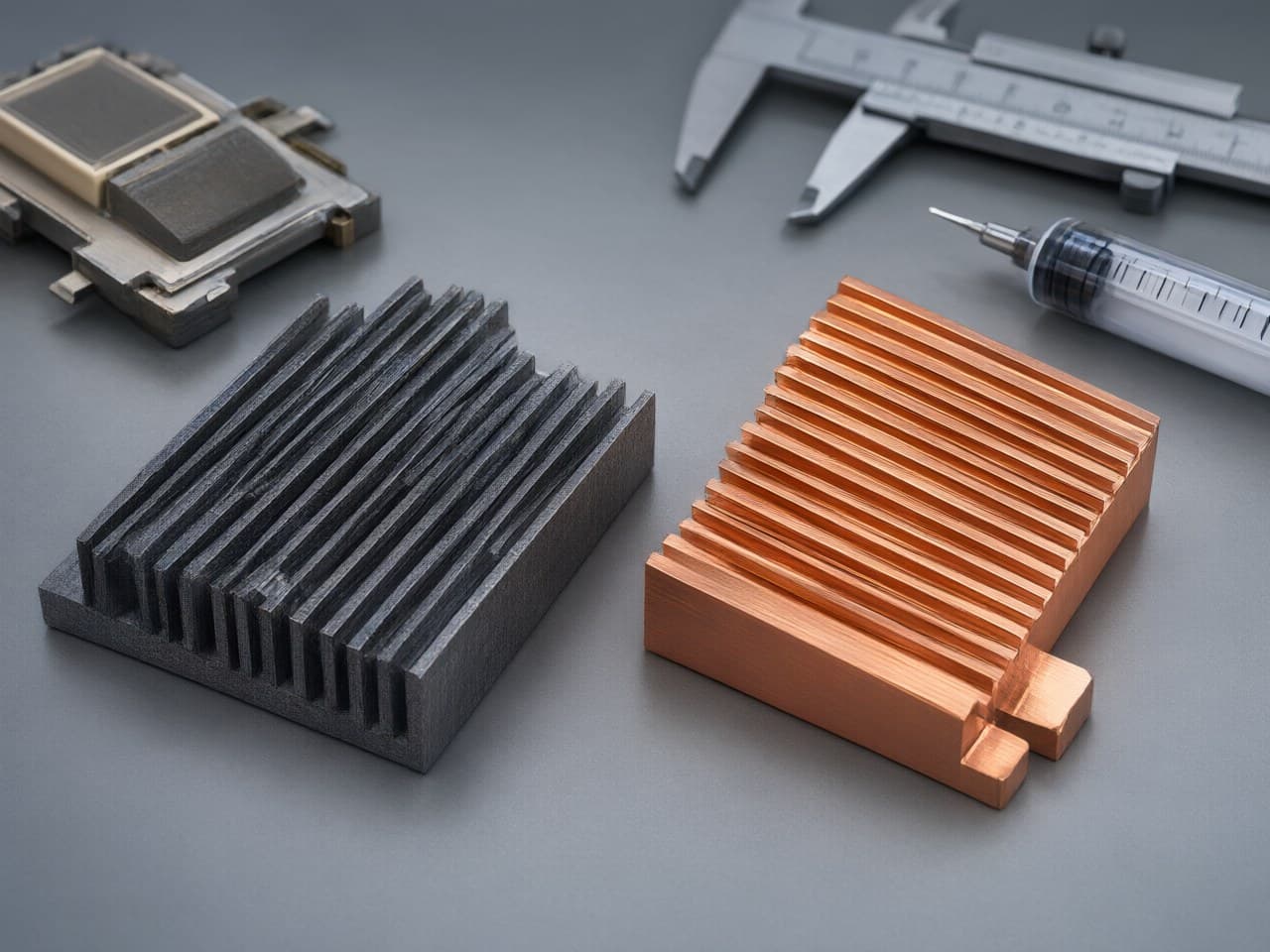
How to Choose Between Tungsten-Copper (W-Cu) and Pure Copper Heat Sink Substrates: The Matching Logic of Thermal Conductivity and CTE
The Core Decision Is Not Just About Thermal Conductivity — It Is About CTE-Driven Reliability
Every thermal engineer knows that pure copper delivers the highest thermal conductivity among common packaging metals — roughly 390–400 W/m·K. Yet the failure mode that ends a product's service life is rarely insufficient heat removal at time zero. It is the cumulative fatigue at solder joints, die-attach interfaces, and ceramic-to-metal bonds caused by repeated thermal cycling against mismatched coefficients of thermal expansion (CTE). That tension is why the tungsten-copper versus pure copper substrate decision is one of the most consequential DFM choices in power electronics, RF modules, and semiconductor packaging.
Pure copper's CTE sits near 17 ppm/°C. Alumina (Al₂O₃) substrates are around 7 ppm/°C; aluminum nitride (AlN) around 4.5 ppm/°C; GaN and SiC die materials typically fall in the 3.2–5.6 ppm/°C range (including crystallographic anisotropy). The mismatch between copper and these ceramics or compound semiconductors is large enough to drive warpage, solder cracking, and delamination under high-reliability thermal cycling. Tungsten-copper composites (W-Cu) let the designer move CTE downward by adjusting the tungsten-to-copper ratio, bringing the substrate closer to the die and ceramic carrier.
W-Cu Compositions Trade Peak Thermal Conductivity for a Tunable CTE Match Against Pure Copper
The following table summarizes key thermal and mechanical properties for the most commonly specified compositions. Thermal conductivity and CTE for W-Cu are composition-dependent; the ranges are literature values for fully dense material, not a substitute for incoming inspection on a given lot.
| Property | Pure Copper | W70Cu30 | W80Cu20 | W90Cu10 |
|---|---|---|---|---|
| Thermal conductivity (W/m·K) | 390–400 | ~190–210 | ~170–190 | ~140–170 |
| CTE (ppm/°C, 20–200 °C) | ~17 | ~9–10 | ~7–8 | ~5–6.5 |
| Density (g/cm³) | 8.9 | ~14.5 | ~15.6 | ~16.8 |
| Flexural / yield strength | Moderate | High | Very high | Very high |
| CTE match to AlN / GaN / SiC | Poor | Good | Very good | Excellent |
| CTE match to Al₂O₃ | Poor–Fair | Very good | Good | Tighter than needed |
| Relative material cost | Low | Moderate–High | High | High |
What this means for design decisions: When the die or substrate is a compound semiconductor (GaN, SiC) or AlN ceramic, W80Cu20 or W90Cu10 provides the closest CTE match and is the usual starting point for solder-joint fatigue life. When the carrier is Al₂O₃, W70Cu30 often hits the practical sweet spot. Pure copper remains the right choice when the assembly uses compliant die-attach materials, operates in mild thermal-cycling environments, or when absolute peak thermal conductivity is the overriding constraint.
Interface Stress Scales with CTE Mismatch, Which Is Why Composition Choice Drives Fatigue Risk
The thermoelastic stress at a bonded interface between two materials can be approximated by:
where Δα is the CTE difference between substrate and die/ceramic (in 1/°C, i.e. ppm/°C × 10⁻⁶), ΔT is the temperature excursion during operation or reflow, E_eff is an effective modulus accounting for the solder or die-attach interlayer, and ν is Poisson's ratio. This is a first-order biaxial estimate; it does not replace finite-element analysis or qualification testing.
What this tells the designer: Interface stress scales linearly with CTE mismatch. Reducing Δα from about 10 ppm/°C (copper on AlN, order-of-magnitude) to about 3 ppm/°C (W80Cu20 on AlN) cuts that first-order driving force by about two-thirds. For a ΔT on the order of 150 °C in a power-cycle profile, that is often the difference between early interface cracking and a joint that can be designed to high-reliability cycling profiles. Actual life still depends on solder composition, geometry, and dwell time. The trade-off is on the order of a 50 % reduction in bulk thermal conductivity versus pure copper, which must be recovered in geometry — thinner substrates, micro-channels, or finned structures.
Pure Copper and Tungsten-Copper Each Win Only Inside a Defined Design Window
Pure copper is preferred when:
- The thermal path is short and the dominant resistance is at the heat-sink-to-ambient interface, not at the die-attach layer. - The assembly uses soft, compliant die-attach (e.g., indium solder, thermal grease) that can absorb CTE-mismatch strain. - Operating temperature swings are mild (ΔT < 40–60 °C) and total cycle counts are low. - Maximum thermal spreading is needed — e.g., optical transceiver heat spreaders where warpage is managed by thin-section design.
Tungsten-copper (W70Cu30 or W80Cu20) is preferred when:
- The die material is GaN, GaAs, or SiC and the substrate is AlN or BeO — all low-CTE materials. - Hard solders (AuSn, AuGe) are used for hermetic or high-reliability die-attach, leaving little compliance to absorb mismatch. - The product must survive MIL-STD or AEC-Q type thermal-cycling profiles (commonly on the order of –55 °C to +150 °C, 1 000+ cycles — confirm the exact condition in the governing specification). - Dimensional stability and flatness must be held over the product's lifetime — critical for RF power amplifier modules and laser diode submounts. - Hermetic packaging needs a shell or lid with CTE-matched flanges to limit seal leakage.
MIM Near-Net W-Cu Pays Off Only When Density, Carbon, Shrinkage, and Part Size Stay Inside Process Limits
MIM/PM near-net-shape processing for W-Cu substrates can cut difficult machining of W-Cu and integrate features that infiltration-plus-machining would have to mill from a blank. Engineers should still treat the following as hard process limits, not footnotes.
Density sensitivity. W-Cu thermal conductivity is strongly dependent on sintered density. Below ~97 % relative density, residual porosity degrades thermal conductivity disproportionately because pores act as thermal insulators. Achieving relative density ≥ 98 % — Newlife - MIM's published near-net-shape control level — is essential if the part is to approach the literature conductivity range for its composition.
Carbon control. Residual carbon from binder burnout can form tungsten carbide at grain boundaries, reducing both thermal conductivity and ductility. Debinding atmosphere control and sintering-profile discipline are non-negotiable.
Shrinkage uniformity. W-Cu parts typically shrink ~15–20 % linearly during sintering. Non-uniform wall thickness or abrupt cross-section changes amplify differential shrinkage, leading to warpage or cracking. DFM review should target uniform wall sections and gradual transitions.
When MIM is not the best fit:
- Very large substrates (> 50–80 mm in any dimension) where shrinkage-tolerance accumulation exceeds ±0.3–0.5 % of the nominal dimension. - Ultra-thin substrates (< 0.3 mm) that are better served by tape-casting or rolled sheet. - Single-digit prototype quantities where CNC from wrought W-Cu billets may be faster and cheaper than tooling investment. - Designs that need the absolute peak conductivity of fully dense pure copper and can tolerate copper's CTE with a compliant attach.
Powder PSD, Sintered Density, and Surface Finish Determine Whether a W-Cu Substrate Meets the Datasheet
For procurement teams evaluating W-Cu substrate suppliers, three audit checkpoints matter most.
Powder and feedstock control. Newlife - MIM develops proprietary ultra-fine copper, iron, and nickel powders (D50 ≤ 3 μm) and custom MIM feedstocks in-house, with tungsten-copper among the production material systems. Control of powder particle-size distribution is the largest practical lever for uniform sintered density and low residual porosity — and therefore for the thermal conductivity the customer actually receives.
Sintered density verification. Newlife - MIM's near-net-shape control targets relative density ≥ 98 %, which is the density floor that W-Cu heat sinks, substrates, heat spreaders, and electronic packaging shells need if conductivity is to track the composition table above. Common packaging compositions such as W70Cu30 and W80Cu20 cover the CTE window most often required for semiconductor and RF stacks. For pure copper and copper-alloy MIM thermal parts, the published sintered-density floor is ≥ 8.4 g/cm³.
Surface compatibility and downstream processing. Substrates can be specified for Ni/Au and Ni/Ag electroplating, vacuum brazing, soldering, wire bonding, and mirror-finish lapping, so they drop into standard semiconductor packaging flows after the finishes the package already requires.
Complex geometry capability. MIM near-net-shape forming enables micro-channels, micro-fins, stepped cavities, and multi-level structures that are expensive to machine from solid W-Cu billets. That matters for high-power-density layouts (GaN HEMTs, SiC MOSFETs, high-power laser arrays) where integrated micro-channel cooling in the substrate is a design option, not a machining afterthought.
CTE Matching Is Becoming More Critical as Wide-Bandgap Devices and Hard Solders Spread
Three converging trends are shifting high-performance thermal substrates toward W-Cu and away from pure copper:
1. Wide-bandgap semiconductor adoption. GaN and SiC devices run at higher junction temperatures and higher power densities than silicon, raising both ΔT and the cost of CTE mismatch. 2. Hard-solder die-attach for reliability. AuSn and sintered-silver die-attach — increasingly specified for automotive and aerospace — offer near-zero compliance, so CTE matching is the remaining lever on interface stress. 3. Miniaturization and 3D packaging. Smaller die and tighter pitch reduce the solder-joint area available to distribute stress, amplifying any remaining CTE mismatch.
Pure copper will continue to serve high-volume, cost-sensitive, moderate-reliability applications. For the growing segment of high-reliability, high-power-density electronics, W-Cu substrates made by MIM/PM near-net-shape processes are the scalable path to CTE-matched thermal management.
These Four Next Steps Will De-Risk the W-Cu Versus Pure Copper Decision
1. Map your CTE chain. List every material in the thermal stack — die, die-attach, substrate, carrier, heat sink — and their CTEs. The largest mismatch interface is where the W-Cu vs. copper decision has the most impact. 2. Define your thermal-cycling profile. Quantify ΔT, cycle count, and dwell time. If the qualification standard demands hundreds of cycles at ΔT > 100 °C with hard solder, W-Cu should be the baseline. 3. Evaluate geometry complexity early. If the substrate needs micro-channels, stepped cavities, or thin-wall features, compare MIM near-net-shape cost against CNC from billet before the outline drawing freezes. 4. Request a DFM review and rapid prototype from Newlife - MIM. Visit www.newlife.cn to connect with the Newlife - MIM application engineering team for a consultation, CTE-matching analysis, and custom W-Cu or pure copper substrate engineering support tailored to your die, package, and reliability requirements.
References
1. ASM International, ASM Specialty Handbook: Copper and Copper Alloys, ASM International, 2001. 2. German, R. M., Sintering Theory and Practice, Wiley-Interscience, 1996. 3. Johnson, R. W., et al., "The Changing Automotive Environment: High-Temperature Electronics," IEEE Transactions on Electronics Packaging Manufacturing, vol. 27, no. 3, 2004. 4. JEDEC Standard JESD22-A104, "Temperature Cycling," JEDEC Solid State Technology Association. 5. Newlife - MIM official product pages: Tungsten-Copper Heat Sinks, W-Cu Substrates, Chip Heat Sink Bases, Copper Thermal Packaging Components — www.newlife.cn.